
AP_01 // BATTERY PACK
Thermal gap-fill between cells
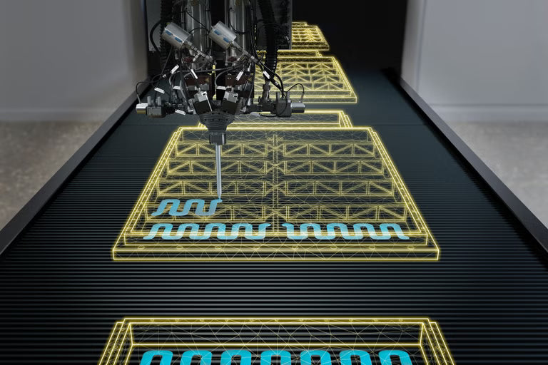
Gap-filling compound dispensed into the space between cells to move heat into the housing while cushioning against vibration — placement and bead volume tuned to the pack geometry.
One engineering partner from material selection through mass production — bonding, sealing, potting and thermal management for high-mix electronics.
• IND // BY INDUSTRY
Application-specific bonding, sealing and thermal recommendations, mapped to the assembly challenges of each industry.
 Consumer electronics
Micro-gap sealing, IPX waterproofing and acoustic-safe adhesives — matched to automated dispensing for high-mix lines.
View solutions Medical devices
Device bonding and skin-contact assembly with medical-grade, biocompatibility-focused material selection.
View solutions EV & energy storage
Cell bonding, thermal interface, pack sealing and structural gap-fill for battery systems.
View solutions Power electronics
Encapsulation, potting, thermal management and dielectric protection for power modules.
View solutions Precision manufacturing
Tight-tolerance bonding, low-outgassing chemistry and repeatable dispensing process.
View solutions Automotive
Structural bonding, vibration damping and environmental sealing for demanding duty cycles.
View solutions• APP // WHERE THE BONDS GO
The joints we design for — where material, gap and process meet on a real assembly.
AP_01 // BATTERY PACK
Gap-filling compound dispensed into the space between cells to move heat into the housing while cushioning against vibration — placement and bead volume tuned to the pack geometry.

AP_02 // PCB STAKING
Beads placed to lock tall components and protect the board against moisture and shock, without bridging pads or interfering with rework — a dispensing pattern qualified to your line.

AP_03 // NARROW BEZEL
Shadowed bond lines under a slim bezel need chemistry that stays workable, then fully cures — the classic case for UV delayed-cure, matched to the substrate and the cure window.

AP_04 // ENCAPSULATION
Full encapsulation for isolation, heat path and environmental sealing — with attention to exotherm, flow into tight windings and stress on delicate parts as it cures.
• PROC // FULL-LINK
The full-link engineering path — the same team from first review to production ramp, so nothing is lost in a handoff.
Joints, substrates and constraints assessed against the application.
Chemistry matched to substrate, gap, cure and service environment.
Bead, fixture and placement trialed on representative parts.
Cure profile tuned for throughput without weakening the bond.
Performance verified under your real production conditions.
Process transferred to the line with ongoing technical support.
• FAQ
Both, but the engineering comes first. We select and pair materials from lines like Henkel, Loctite, 3M and Dow, then develop the dispensing, curing and validation process so the material actually works on your line.
Yes. We tune bead, fixture, placement and cure profile to your equipment and takt, and validate under your real conditions before scale-up.
Consumer electronics, medical devices, EV and energy storage, power electronics, precision manufacturing and automotive. Pick your industry above for application-specific detail.
Tell us your substrates and bond points. An application engineer will review them with you and propose a material and process path.
We'll review them with you and propose a material and process path — from prototype to production.